
Optimizing Thermal Relief Pads for Better Heat Dissipation and Reliable Soldering
14 min
- What Thermal Relief Pads Are and Why They Are Used
- Key Benefits of Proper Thermal Relief Pad Design
- Design Considerations for Effective Thermal Relief Pads
- Common Design Mistakes and How to Avoid Them
- Manufacturing Aspects and Quality Assurance
- JLCPCB's Expertise in Thermal Relief Pad Implementation
- FAQ about Thermal Relief Pad
- Conclusion
Key Takeaways
- Prevent Solder Defects: Relief spokes trap heat to stop cold joints and prevent tombstoning on small parts.
- Skip Power Pads: Keep thermal pads and >3A traces solid for maximum heat escape and minimal voltage drop.
- Match Spoke Geometry: Use thin spokes (0.10–0.20) for passives and wider spokes (0.20–0.30mm}) for standard SMD.
- Add Etch Margin: Size spokes 30% over fab minimums to survive over-etching during production.
You have probably never changed a thermal relief pad setting in your life. Your design tool picked a spoke width the day you installed it, and every ground pin on every board since has quietly used that number. If there is too much copper in the thermal relief pad, your iron cannot heat the joint, so you get a cold joint that fails six months into the field. And on the other hand, if there is too little copper, the power pad runs hot or drops voltage, you cannot spare. This guide explains what the spokes actually do, which widths and gaps suit which parts, when to skip relief entirely, and how fabrication tolerance changes the copper you drew.
What Thermal Relief Pads Are and Why They Are Used
Definition and Role in Connecting Pads to Copper Planes
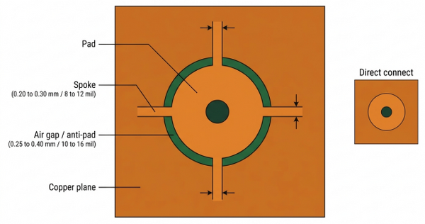
A thermal relief pad connects a pad to its copper plane through a few narrow arms instead of solid copper. Those arms are the spokes, and the ring of bare board around them is the air gap, or anti-pad. Electrically, the pad is still tied to the plane. Thermally, it is throttled.
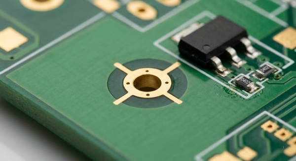
Let’s take an example of a saucepan handle. It bolts to the pot through a thin steel neck, and that neck is why you can lift the pot without burning your hand. Weld it flat to the pot body, and it gets as hot as the water inside. A thermal relief pad is that neck, in copper. The heat transfer of copper is approximately 400 W/mK, and of FR4 is approximately 0.3 W/mK, so any large copper pour is a thousand times more efficient at removing heat from a joint than the board underneath.
The Balance Between Heat Dissipation and Solderability
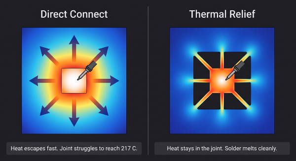
Solder only flows once the joint passes its melting point. Leaded Sn63/Pb37 melts near 183 C and lead-free SAC305 needs about 217 C, so ovens peak at 235 C to 250 C for margin. That has to happen at the pad, not in the air above it. Drop that pad onto a 2 oz ground plane, as on the driver board inside a mains LED bulb, and the plane pulls heat sideways while you try to heat the joint. A 60 W hand iron can lose that race outright, and a wave machine has seconds to win it.
So the pad has two opposing jobs: to shed heat quickly during operation, and hold it in while soldering. Spoke width sets the trade.
Key Benefits of Proper Thermal Relief Pad Design
Effective Thermal Management for High-Power Components
Here is the part that surprises people. For a genuinely hot component, the best thermal relief setting is usually none at all.
Example: Take an AMS1117-3.3 regulator in an SOT-223 package, or an LM2596 buck converter in a TO-263 tab package. Heat from the silicon has one escape route: through the metal tab, into the pad, into the plane, out across the board. Spokes sit in that route, so cutting a solid connection to four arms of 0.3 mm (12 mil) strips out most of the copper the heat was using. The skill is knowing which pads to relieve. Signal and low-current ground pins benefit, since they carry milliamps and only need to be soldered cleanly. Tabs and exposed pads stay solid because moving heat is their whole purpose.
Improved Soldering Quality and Reduced Tombstoning Risk
Tombstoning is when a small two-terminal part stands upright on one end during reflow, leaving the other end in the air and the circuit open. It is among the most common defects on the 0402 and 0603 parts packed into a phone charger, and copper imbalance is a leading cause.
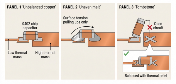
One end of a 0402 capacitor lands on a wide ground pour, the other on a 0.2 mm (8 mil) trace. The pour end has more copper attached, so it heats more slowly and melts later. The trace end melts first and pulls hard with surface tension, and the part pivots upright. Relief on the pour end equalizes the heating.
Design Considerations for Effective Thermal Relief Pads
Spoke Width, Number of Spokes, and Clearance Settings
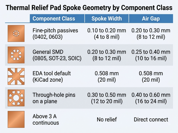
Three numbers define a thermal relief pad: spoke width, gap width, and spoke count. IPC-2221B puts the practical floor for spoke width at 0.2 mm (8 mil) and treats four spokes as the normal maximum. Four is what nearly every tool generates, and what you should use.
| Component Class | Spoke Width | Air Gap | What It Does for You |
|---|---|---|---|
| Fine-pitch passives (0402, 0603) | 0.10 to 0.20 mm (4 to 8 mil) | 0.20 to 0.30 mm (8 to 12 mil) | Stops tombstoning |
| General SMD (0805, SOT-23, SOIC) | 0.20 to 0.30 mm (8 to 12 mil) | 0.25 to 0.40 mm (10 to 16 mil) | Easy hand rework |
| Through-hole pins on a plane | 0.30 to 0.50 mm (12 to 20 mil) | 0.40 to 0.60 mm (16 to 24 mil) | Barrel reaches melting point |
| Any pad above 3 A continuous | None, direct connect | Not applicable | Low resistance and drop |
Small parts need thin spokes and tight gaps, pin holes need fat spokes, so there's still copper to conduct, and high-current pads are best to be avoided entirely. Altium's default is 0.2mm (8 mil) spokes/clearance for most parts, and KiCad is defaulting to 0.508mm (20 mil) for both.
Component Type, Power Level, and Board Thickness Influence
Start with how the board will be soldered. Hand soldering is the harshest, since one iron tip must beat a whole plane. Wave soldering is next, with seconds of contact per joint. Reflow is gentlest, because the board heats evenly, so relief matters far less on a surface-mount design.
A four-spoke relief with 0.25 mm (10 mil) arms lands around 1 to 3 milliohms per pad, so at 5 A, you lose 5 to 15 mV and turn 25 to 75 mW into heat there. Past 3 A continuous, switch to a solid connection, and fix soldering with preheat.
Thickness works the same way: A 2.0 mm (79 mil) board with two internal planes is the worst case for barrel fill, while a 1.0 mm (39 mil) two-layer board is the easiest. Internal planes also hide the problem, since a pin can look relieved on the outer layer and still be tied solidly to two buried sheets.
Interaction with Thermal Vias and Copper Pour Strategies
IPC-7093, the standard covering bottom-terminated parts, calls for a direct copper connection with a via array under a QFN, DFN, or DPAK. That pad is the die's only escape route, and spokes would choke it.
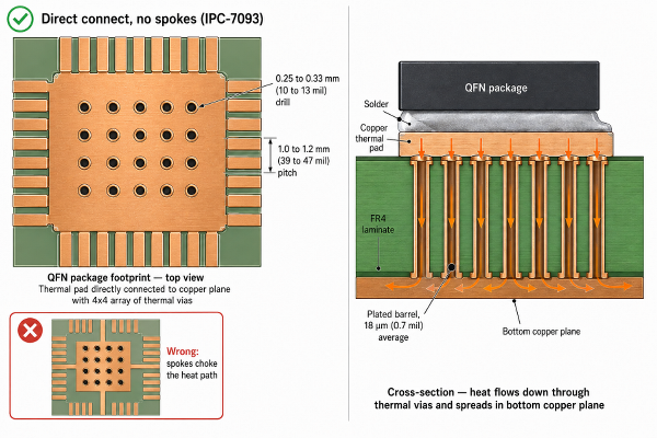
Size the array properly, because it does the work, the spokes are not:
- Drill 0.25 to 0.33 mm (10 to 13 mil) holes: Anything larger wicks solder away during reflow.
- Space them 1.0 to 1.2 mm (39 to 47 mil) apart: Typical arrays run 9 to 25 vias by pad size.
- Tent, plug, or fill them: An open via drains paste downward and leaves a void above it.
- Keep voiding below the IPC-7093 limit of 50%: Voids are trapped air, and air conducts heat about as well as nothing.
Pour strategy matters as much. A pin can be relieved on the top layer where you see it and tied solidly to a buried plane where you do not, and the buried one ruins the joint.
Common Design Mistakes and How to Avoid Them
Overly Strong or Weak Thermal Relief Leading to Soldering Issues
Mistake 1: Leaving the tool's default applied to every pad.
A 0.508 mm (20 mil) spoke is fine on a through-hole connector and clumsy under a 0402, where four fat spokes and their gaps swallow the plane between parts. To fix this: create one relief rule per component class.
Mistake 2: Drawing spokes at the fabrication minimum.
Track width tolerance is typically ±20%, so a 0.10 mm (4 mil) spoke can arrive at 0.08 mm (3 mil) or etch away entirely, leaving an open circuit that no inspection will catch. To fix this: design at least 30% above your fab's stated minimum.
Mistake 3: Relieving the exposed pad under a power package.
Tools apply pour rules to every pad by default, including the thermal pad under a QFN, and the spokes can halve the heat path. To fix this: set exposed pads to direct connect, then inspect the pour.
Poor Integration with High-Current or High-Frequency Designs
Mistake 1: Relieving high-current pads to make assembly easier.
Spokes make a joint solderable and resistive at once. On a 10 A pad, a relief adding 3 milliohms burns 300 mW right there. To fix this: keep high-current pads solid and solve soldering with preheat.
Mistake 2: Putting relief on ground vias and shield pins in high-speed designs.
Return current follows the signal and needs a low-inductance path back through the plane. Spokes squeeze it through four narrow arms, adding inductance where you wanted to remove it. To fix this: exclude vias from relief rules and direct-connect the connector and shield-can grounds.
Mistake 3: Relieving the ground pad of an RF component.
On a radio module such as an ESP32-WROOM-32, the pad underneath is both a heat path and the RF reference plane. To fix this: treat any RF reference pad as a direct connect.
Manufacturing Aspects and Quality Assurance
Etching Precision, Solder Mask Alignment, and Process Controls
Your spokes are the narrowest copper on the board, so they suffer first when a process drifts. Etching removes copper sideways as well as downward, and that shortfall is a far bigger percentage of a 0.15 mm (6 mil) spoke than of a 1 mm (39 mil) power trace.
| Process Parameter | Typical JLCPCB Capability | What It Does to Your Relief |
|---|---|---|
| Track width tolerance | ±20% | A drawn 0.20 mm (8 mil) spoke can arrive at 0.16 mm (6.3 mil) |
| Min trace and space, 1 oz multilayer | 0.09 / 0.09 mm (3.5 / 3.5 mil) | The absolute floor for a spoke, so never design to it |
| Min trace and space, 2 oz outer | 0.16 / 0.16 mm (6.5 / 6.5 mil) | 2 oz undercuts more, so it needs wider spokes than 1 oz |
| Solder mask expansion | 1:1, min 0.09 mm (3.5 mil) between openings | Stops mask slivers from flaking off around the relief gap |
| Annular ring | 0.20 mm (8 mil) or greater | The ring is where the spokes attach |
| Hole plating | 18 µm (0.7 mil) average | Carries solder to heat up the barrel and helps it fill |
To summarise, the copper that you receive will always be thinner than the copper that you drew, and whether or not the gap around your pad remains clean will depend on mask registration.
Testing Methods for Thermal Performance Validation
Checking that a thermal relief pad works means looking inside joints and measuring temperature. Six methods give a real answer:
- Microsection the joint: This cross-section of a through-hole pin reveals the extent to which the solder advanced up the barrel as compared to the 75% fill requirement of J-STD-001.
- X-ray bottom-terminated parts: The voids beneath a QFN or DPAK pad are not visible from the outside, and are restricted by IPC-7093 to be not more than 50% of the pad area.
- Perform a thermocouple profile: Tape thermocouples to a relieved and an unrelieved pad on a scrap board and reflow it. The relief is effective if the relieved pad melts earlier.
- Take a thermal camera image under load: A gap of over 10 C to 15 C against simulation means copper is missing somewhere.
- Thermal cycle sample: IPC-9701 covers cycling for surface-mount solder attachment reliability, and it is where starved barrels crack.
- Electrically test every board: Flying probe catches a spoke that etched away completely, the one defect that looks perfect under a microscope.
JLCPCB's Expertise in Thermal Relief Pad Implementation
Advanced DFM Review Optimized for Thermal and Soldering Performance
Every order runs through an automated design-for-manufacturing check before reaching the production floor, and you can run the same check yourself with JLCDFM before committing. It flags copper features falling below process minimums, which is exactly the failure mode that kills thin spokes.
Use it specifically on relief geometry. A spoke below 0.09 / 0.09 mm (3.5 / 3.5 mil) on a 1 oz multilayer board, or below 0.16 / 0.16 mm (6.5 / 6.5 mil) on 2 oz outer copper, passes your own design rule check and still cannot be etched reliably. Catching that before fabrication costs nothing, and catching it after costs a build.
Reliable High-Quality Production for Thermal-Critical Boards
Boards that push heat need options beyond a standard 2-layer stackup: 1 to 32 layers, finished thickness from 0.4 mm to 4.5 mm (16 mil to 177 mil), and outer copper up to 4.5 oz on 2-layer boards. Heavier copper lets you carry more current through fewer spokes, or skip relief entirely and still hand-solder comfortably.
If you are assembling as well as fabricating, the same board goes straight into SMT assembly with parts from the component library. That matters here because the people setting the oven profile can see the copper you drew.
FAQ about Thermal Relief Pad
Q: What is a thermal relief pad?
It connects a pad to its copper plane through a few narrow spokes instead of solid copper. The spokes hold the electrical connection while throttling heat escape, which makes the pad far easier to solder.
Q:Do surface-mount pads need thermal relief, or only through-hole pins?
Both can. Through-hole pins need it most, since soldering must fight the whole plane to fill the barrel. Surface mount pads need it to balance copper across small passives so they do not tombstone.
Q: What spoke width and gap should I use as a starting point?
Four spokes of 0.20 to 0.30 mm (8 to 12 mil) with a 0.25 to 0.40 mm (10 to 16 mil) gap suits most components, dropping to 0.10 to 0.20 mm (4 to 8 mil) in dense 0402 and 0603 areas. IPC-2221B treats 0.2 mm (8 mil) as the floor.
Q: Should the exposed pad under a QFN or DPAK get thermal relief?
No. IPC-7093 calls for a direct copper connection with a via array, because that pad is the die's only heat path out. Set it to direct connect explicitly, since most tools relieve it by default.
Q: Does thermal relief reduce how much current a pad can carry?
Yes, though it stays small until the current gets large. A four-spoke relief with 0.25 mm (10 mil) arms adds roughly 1 to 3 milliohms, so at 5 A you lose 5 to 15 mV and dump 25 to 75 mW. Above 3 A continuous, use a direct connect.
Conclusion
The useful reframe for a thermal relief pad is that you are not choosing between good and bad. You are choosing which few seconds of the board's life to optimize for. Spokes buy a clean joint during soldering and cost you heat flow and current capacity for the decade afterward. Signal pads happily make that trade. Power tabs, exposed pads, and high-current rails never should. So inspect the poured copper before you export, not just the routing. Most relief failures are visible in five seconds at that stage and invisible forever after. When your copper is settled, JLCPCB's DFM review and tight etch tolerances make sure the spokes on the finished board match the ones on your screen.

Popular Articles
• Understanding Digital Circuit Timing: Setup Time, Hold Time, Contamination Delay & Clock Skew
• PCBs Explained: A Simple Guide to Printed Circuit Boards
• Understanding the Basics of Electronic Devices and Circuits
• Choosing the Right Electronic Components for Your Electronic Design: Tips and Best Practices
• Guide to the Top 10 Commonly Used Electronic Components
Keep Learning
Optimizing Thermal Relief Pads for Better Heat Dissipation and Reliable Soldering
Key Takeaways Prevent Solder Defects: Relief spokes trap heat to stop cold joints and prevent tombstoning on small parts. Skip Power Pads: Keep thermal pads and >3A traces solid for maximum heat escape and minimal voltage drop. Match Spoke Geometry: Use thin spokes (0.10–0.20) for passives and wider spokes (0.20–0.30mm}) for standard SMD. Add Etch Margin: Size spokes 30% over fab minimums to survive over-etching during production. You have probably never changed a thermal relief pad setting in your li......
Electronic Devices and Circuits
Key Takeaways Components: Passive (resistors, capacitors, inductors) manage energy; Active (transistors, ICs) control signals. Accuracy: Inductors exhibit inductive reactance (XL); MOSFETs are voltage-controlled power switches. PCB Specs: JLCPCB delivers 1–32 layers, 3.5/3.5 mil trace/space, and 0.2 mm min via. SMT Capability: PCBA handles 0201/0402 parts with AOI/X-Ray quality control. In the realm of modern technology, electronics devices and circuits play a crucial role in powering everything from ......
Understanding Digital Circuit Timing: Setup Time, Hold Time, Contamination Delay & Clock Skew
It is the second article in the series on propagation delay in digital circuits. There are two main things we have to make sure of when designing a digital circuit: the first is functionality, and the second is timing. we have covered the basic blocks in one article. Because time is nothing but the clock ticks when it comes to electronics. Because everything is based on these clock ticks, it determines the operating frequency, speed, and much more in an electronics circuit. We have seen circuits previ......
PCBs Explained: A Simple Guide to Printed Circuit Boards
Printed Circuit Boards (PCBs) are the essential building blocks behind almost all modern electronic devices. PCBs play an important role in that they provide electrical interconnections between electronic components, rigid support to hold components, and a compact package that can be integrated into an end product. They are the main component in an electronic device that is responsible for form and function, and they allow advanced semiconductors to communicate with each other at very high data rates.......
Understanding the Basics of Electronic Devices and Circuits
In the realm of modern technology, electronic devices and circuits play a crucial role in powering everything from everyday gadgets to complex machinery. Understanding the fundamentals of these components can provide valuable insights into how various electronic systems operate and interact. This blog explores the basics of electronic devices and circuits, their types, functions, and the significance of their design in today's technological landscape. Electronics means the study of the flow of electro......
Optimize PCB Trace Spacing for High-Performance PCBs
Key Takeaways Trace Spacing vs. Clearance: Trace spacing is the edge-to-edge distance between copper conductors on the same layer, while clearance encompasses the broader safety envelope between traces and non-trace features like board edges and mounting holes. The 3W Rule: For high-speed signals, maintain at least 3x the trace width between centerlines (2W edge-to-edge spacing) to reduce crosstalk by up to 70%. IPC-2221 Standards: Industry-standard clearance values depend on voltage levels, altitude,......